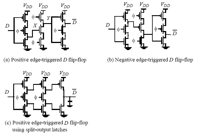
1. how to design the DFF?
2. how to set the input signal for simulation?
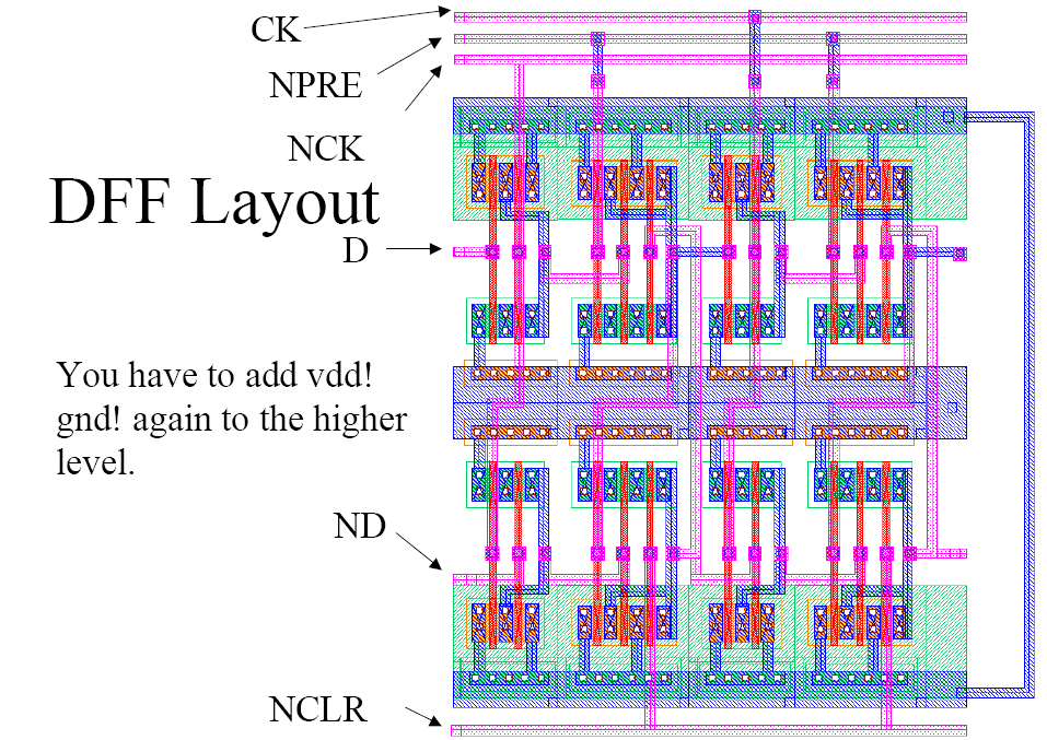
The clock input can be a different metal layer (eg. m2) from the rest of routing metal layer(eg. m1)
Your layout can be even smaller than this one if you choose the schematics in the book or above. Make sure your layout follows the style below so that your design can be as compact as possible. In general the cells should share the same VDD/GND line and should be placed as close to each other as possible.
For more details of the layout below you can go to:
http://www.engr.sjsu.edu/~dparent/ee166
To simulate the DFF, there are two inputs, D and CLK needed to be set. You can set CLK to a period of T and D to 2T in order to show out put flips according to the CLK and D.
One example input setup for Hspice is shown in Notes for HW2. .