Magic Tutorial : Inverter Layout
bug or comment to jsmoon@usc.edu
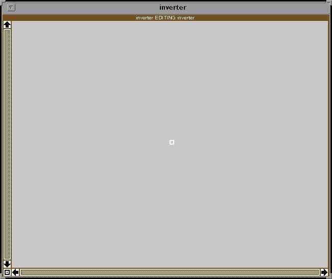
- Execute magic program See Fig
1.
%magic inverter
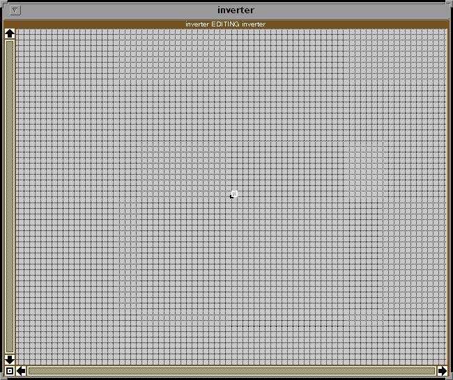
- Show grid on window See Fig
2.
"g" or "box-> :grid"
- "g" : bindkey in magic. Just type "g" while cursor is in the layout
window.
- "box-> :grid" : Type ";" or ":" first, then type grid. There are 4
tools in magic (box,wiring,netlist,rsim).
"box->" means your current
tool is box tool. You can switch between tools by typing "spacebar" key.
- Don't type "box->" Just type ":grid".
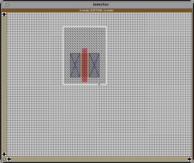
- Draw pmos and nwell See Fig
3.
"box(24,18)-> :paint nwell"
"box(10,12)-> :paint
pdiff"
"box(10,4)-> :paint pdc"
"box(10,4)-> :paint
pdc"
"box(14,2)-> :paint poly"
- "box(24,18)->" : Make a box with height 24 and width 18 by clicking
left mouse button at left bottom point and right mouse button at right top
point.
You can check the box size by typing "b" or ":box".
- ":paint" command can be abbreviated as ":pai". So you can type ":pai
pdiff".
- Don't type "box(24,18)->" Just type ":paint layer".
- At this moment, you have drawn pmos transistor whose W/L is 10/2.
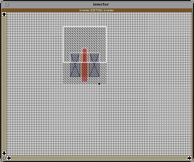
- Increase pmos W from 10 to 12
Sorry!! Your TA should have told
you that W of pmos should be 12. So please follow the next steps.
Step
1: Select part of pmos and nwell. See Fig
4.
click lmb(left mouse button) then rmb(right mouse button) to
make a box as shown in Fig 4.
"a" or "box-> :select"
area
Step 2: Stetch selected area to increase W of pmos.
See Fig
5.
"E" or ":stretch up 1"
"E" or ":stretch up 1"
- Is ":stretch up 2" equivalent to typing "E" twice?? Yes!
- How can you recover pmos with W=10?
- Type "u" twice. ("u" is a bindkey for ":undo")
- Type ":stretch down 2" or "W" twice.
- What is the diffrence between "E" and "e" bindkeys? Check Fig 6
to see the result when you type "e" twice instread of "E".
- What are the white dots in Fig 6? Why do these appear?
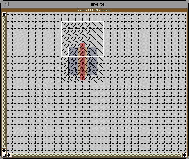
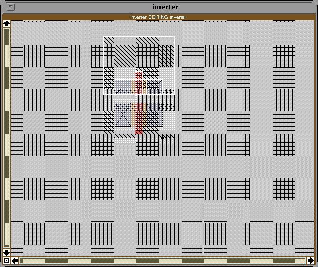
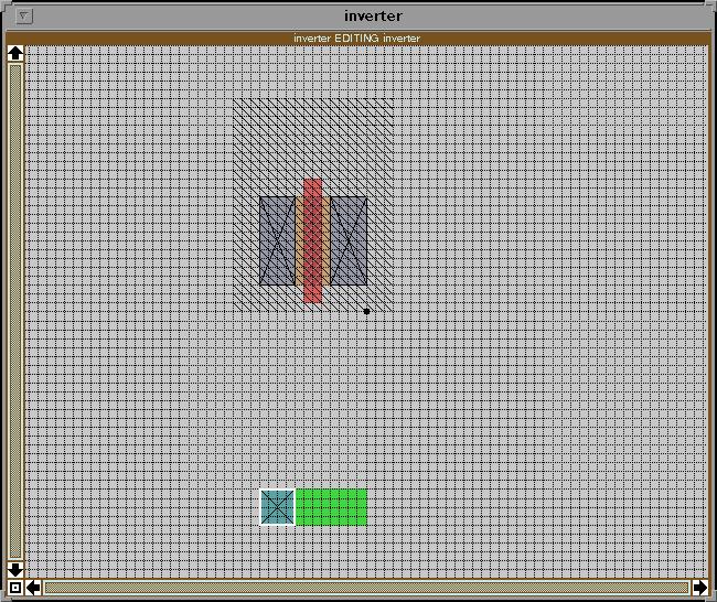
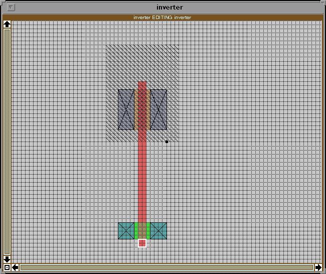
- Draw nmos using copy and wiring tool
Step 1: See Fig
7.
"box(4,12)-> :paint ndiff"
"box(4,4)-> :paint
ndc"
Step 2: See Fig
8.
put cursor on ndc drawn in step 1.
"s" or ":select"
put
cursor on left bottom where selected ndc will be located.
"c" or
":copy"
- Easier and more advanced technique for step 2 is
put cursor on
ndc.
"s"
":copy rignt 4"
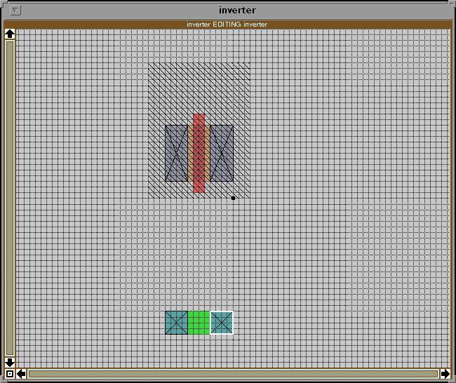
Step 3: Change to
wiring tool by typing "spacebar" key.
- Your command window will display "Switching to "wiring" tool."
- Mouse pointer should switch to arrow type.
Step 4:
See Fig
9.
click lmb on bottom of poly at pmos.
put cursor at the end
point of poly (2 grid below of nmos).
click rmb.
- When you click lmb on bottom of poly, click again if it select nwell
instead of poly.
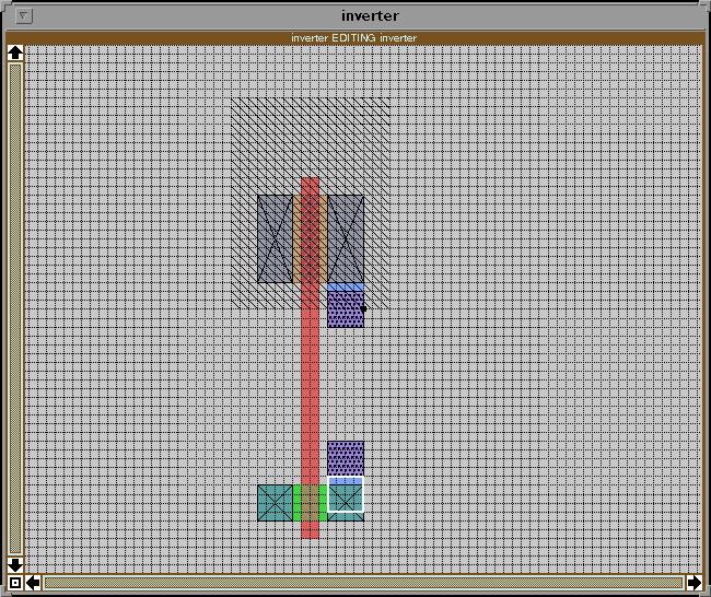
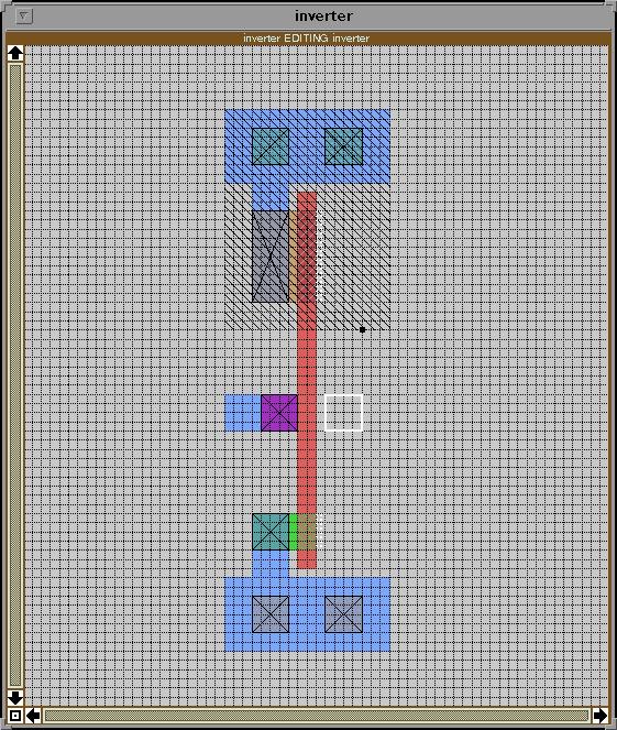
- Draw via and metal1 See Fig
10.
switch to box tool (type "spacebar" key 3
times)
"box(4,4)-> :paint via"
"box(4,4)-> :paint
m1"
"box(4,4)-> :paint via"
"box(4,4)-> :paint m1"
- via is a contact between metal1 and metal2.
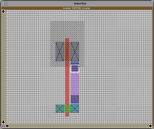
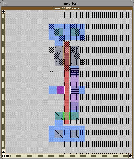
- Draw metal2 See Fig
11.
"box(4,4)-> :paint m2"
switch to wiring tool (type
"spacebar" key)
connect both via by metal2.
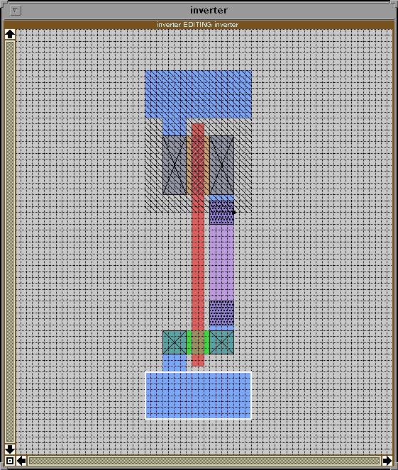
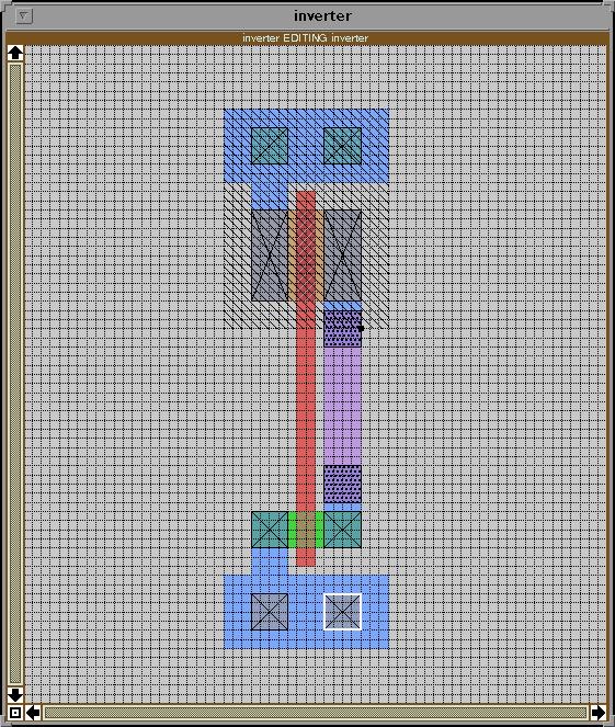
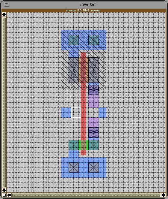
- Draw Vdd and Ground line
Step 1: See Fig
12.
Draw metal1 connections as shown in Fig 12.
Step
2: See Fig
13.
"box(4,4)-> :paint nwc"
"box(4,4)-> :paint
pwc"
- nwc (nwell contact) is a contact between Vdd and nwell.
- pwc (pwell contact) is a contact between Ground and p-substrate.
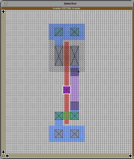
- Draw poly contact and metal1 See Fig
14.
switch to wiring tool
click lmb on the middle of poly
put
cursor on any of metal1
click mmb(middle mouse button) to make a poly
contact
- clicking middle mouse button make a contact between selected layer
(poly) and layer below cursor automatically.
- How can you do the same task within box tool? "box(4,4)-> :paint
pc"
- How can you generate via contact between metal1 and metal2 using the
same technique?
click metal1(or metal2)
put cursor on metal2(or
metal1)
click mmb
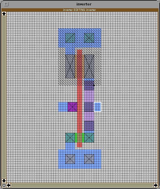
- Finalizing drawing See Fig
15.
Using all techniques you have learned, finalize your layout as
shown in Fig 15.
You may use ":move", wiring and contact generation using
wiring tool.
- Save now
":save"
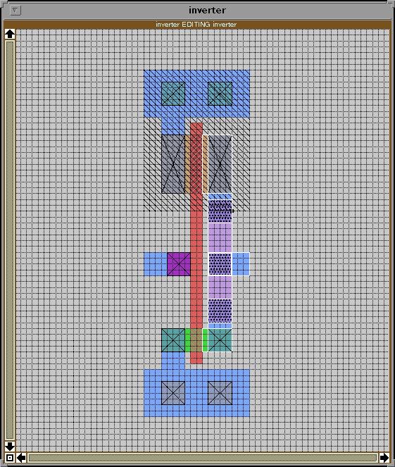
- Delete layer(s)
- Delete selected layers. See Fig
16 and Fig
17.
put cursor on middle via contact
"s"
"s" - This will
select the whole connection with the via.
"d" - This will delete the
whole connection.
"u" - recover by undoing
- Delete selected layers. See Fig
18 and Fig
19.
put cursor on middle via contact
"s"
put cursor on poly
contact
"S" - This will select poly contact while via is selected.
"d"
- This will delete via and poly contact.
"u" - recover by
undoing
- Delete specific layer. See Fig
20 and Fig
21.
"f" - This will show box around the whole cell.
put cursor
on poly
"Ctrl-d" - This will delete only poly layer inside the
box.
"u" - recover by undoing
- "Ctrl-d" is equivalent to ":delete area layer"
- How can you delete poly only in nmos?
make a box around nmos
(click lmb and rmb around nmos)
put cursor on
poly
"Ctrl-d"
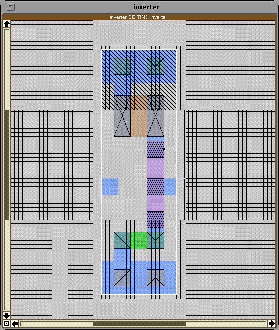
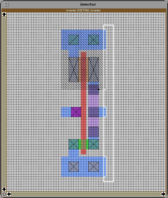
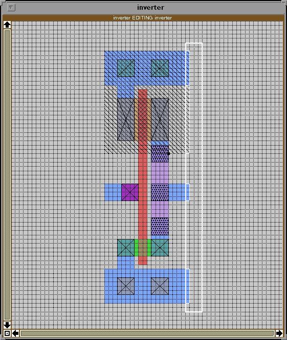
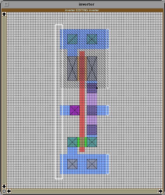
- Enlarge the width of inverter
Your inverter turns out that width
of cell is too small. Let's enlarge it by 2 lambda on both sides.
- By stretch. See Fig
22 and Fig
23.
make a box as shown in Fig 22.
"a" or ":select
area"
":stretch right 2" or "R" twice
- By fill. See Fig
24 and Fig
25.
make a box as shown in Fig 24.
":fill left
2"
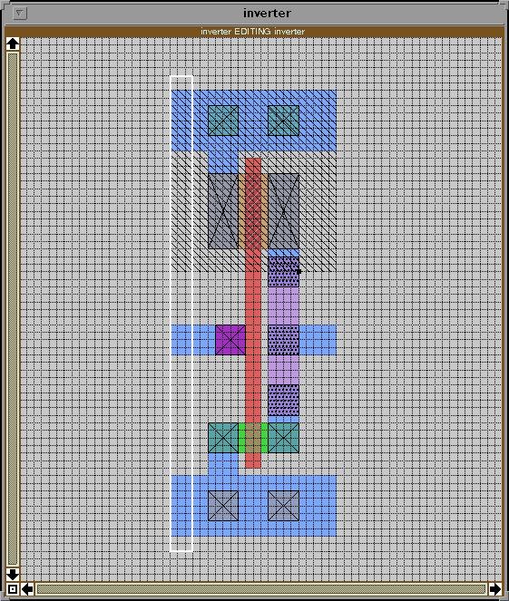
- Labeling
Step 1: See Fig 26
and Fig
27.
put cursor on metal1 of input
click lmb and rmb at the same
point - This will put cross point on metal1.
":label
in"
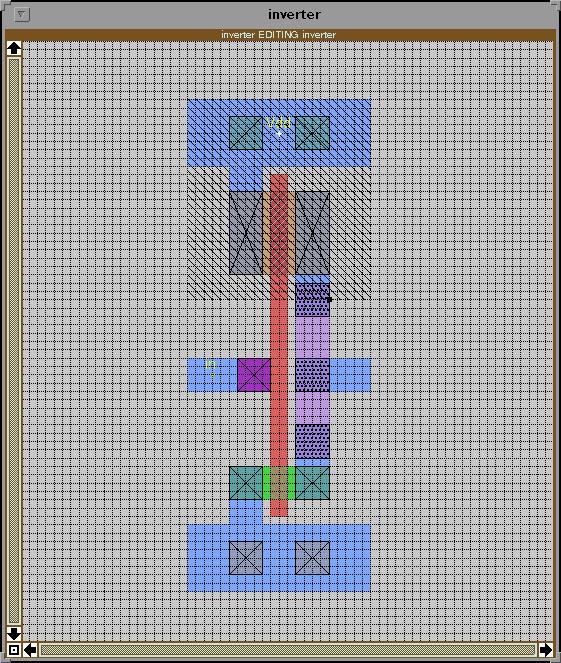
Step 2: See Fig
28.
put cursor on metal1 of Vdd
click lmb and rmb at the same
point
":label Vdd n m1"
- When two layers are overlapped like Vdd (metal1 and nwell), it is always
good practice to specify direction and layer explicitly.
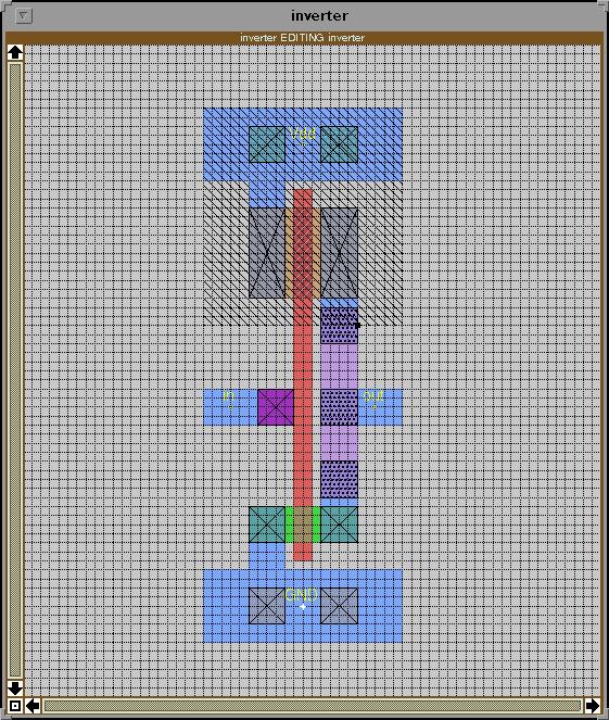
Step 3:
See Fig
29.
Complete labeling as shown in Fig 29.
- Save
":save"
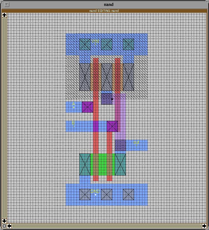
- Practice yourself See Fig
30.
Draw the same nand gate layout shown in Fig 30.
Copyright Joong-Seok "Jay"
Moon
The
University of Southern California does not screen or control the content on this
website and thus does not guarantee the accuracy, integrity, or quality of such
content. All content on this website is provided by and is the sole
responsibility of the person from which such content originated, and such
content does not necessarily reflect the opinions of the University
administration or the Board of Trustees