Section 3 Propagation Delay Analysis of separate parts:
¡¡
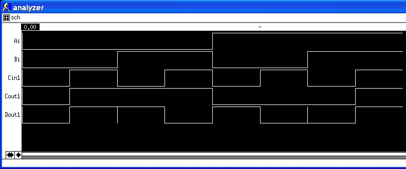
Sub1:
The IRSIM waveform is shown below:
The IRSIM waveform matches the function:
Dout1=Ai¨’Bi¨’Cin1
Cout1=Ai¡¯*Bi + Ai¡¯*C1i + Bi*Cin1
¡¡
According to the IRSIM waveform, we choose the case in which "Ai,Bi,Cin1" change from 000 -> 001-> 000, to measure the propagation delay of Cout1 from the transition of Cin1.
The HSPICE waveform is shown below:
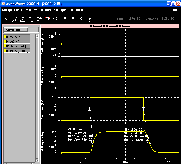
So the propagation delay for Cout1 from transition of Cin1 is: tp=(302+412)/2=357ps
¡¡
¡¡
According to the IRSIM waveform, we choose the case in which "Ai,Bi,Cin1" change from 100 -> 101-> 100, to measure the propagation delay of Dout1 from the transition of Cin1.
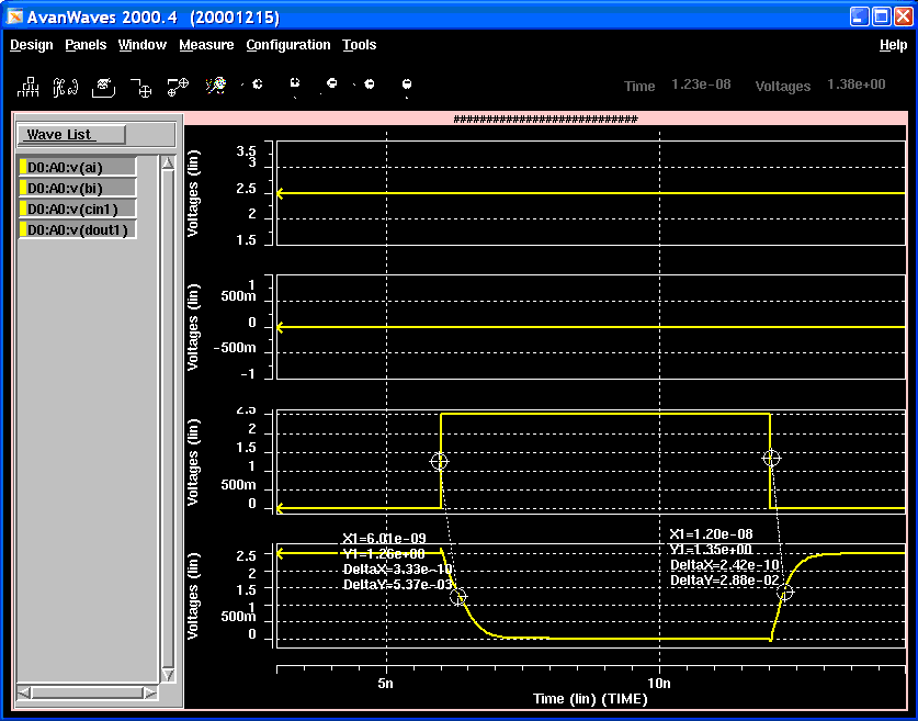
The HSPICE waveform is shown below:
¡¡
So the propagation delay for Dout1 from transition of Cin1 is: tp=(333+242)/2=287.5ps
¡¡
The structure of Sub2 is identical to Sub1, so we may think the propagation delay is the same as Sub1.
¡¡
¡¡
Comparator:
The IRSIM waveform is shown below. It meets the function:
Dout3=Bi¡¯*Ai + Bi¡¯*Cin3 + Ai*Cin3
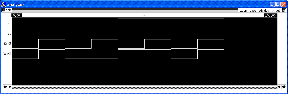
According to the IRSIM waveform, we choose the case in which "Ai,Bi,Cin1" change from 000 -> 001-> 000, to measure the propagation delay of Dout3 from the transition of Cin3.
The HSPICE waveform is shown below:
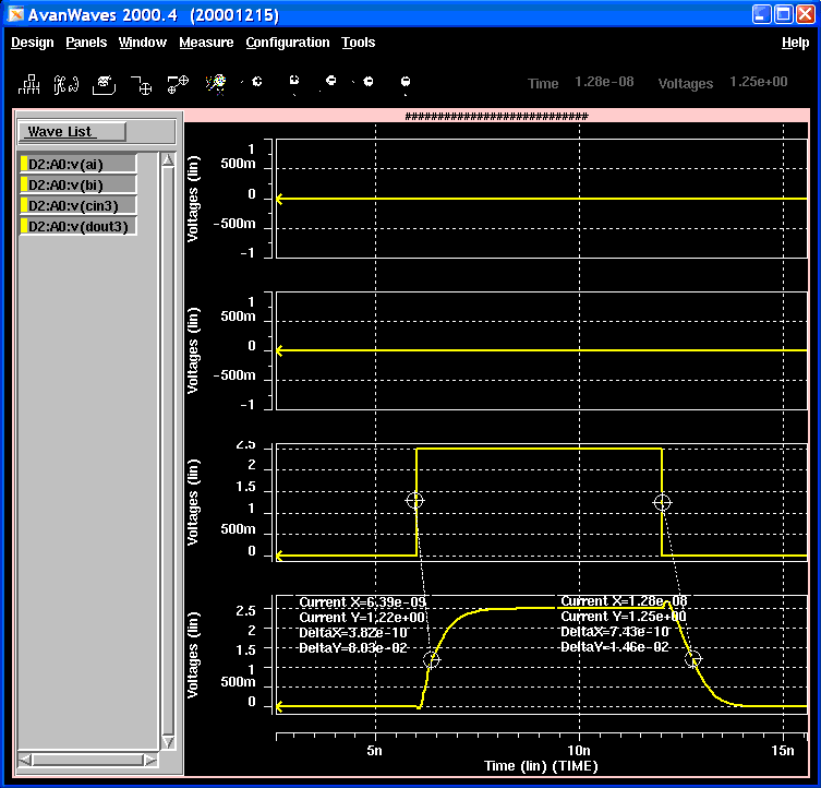
So the propagation delay for Dout3 from transition of Cin3 is: tp=(382+743)/2=562.5ps
¡¡
¡¡
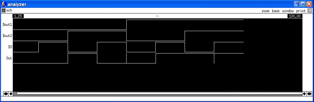
MUX:
The IRSIM waveform is shown below. It meets the function:
Out = Dout2*D3'+ Dout1*D3
¡¡
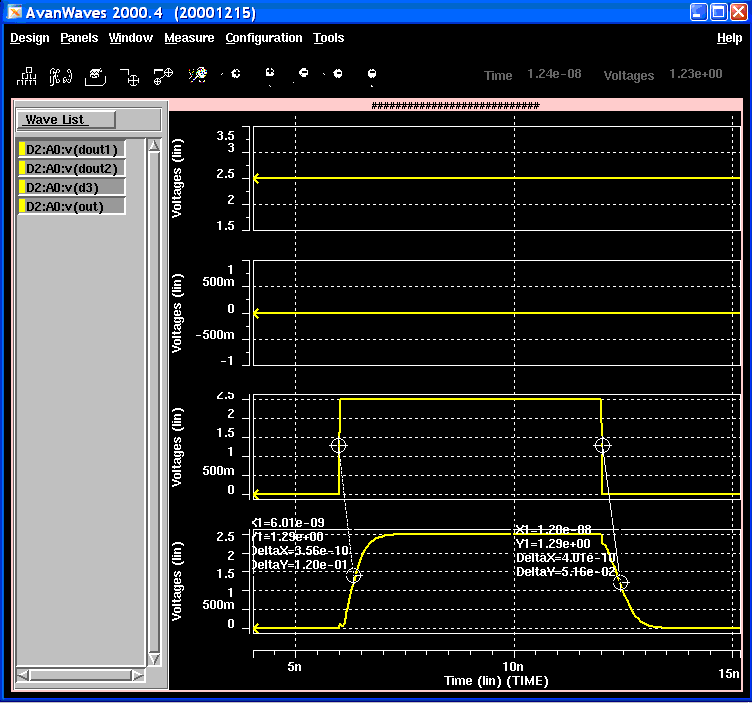
According to the IRSIM waveform, we choose the case in which "Ai,Bi,Cin1" change from 100 -> 101-> 100, to measure the propagation delay of Cout1 from the transition of Cin1.
The HSPICE waveform is shown below:
¡¡
So the propagation delay for Out from transition of D3 is: tp=(356+401)/2=378.5ps
¡¡
The propagation delay from the edge of reset:
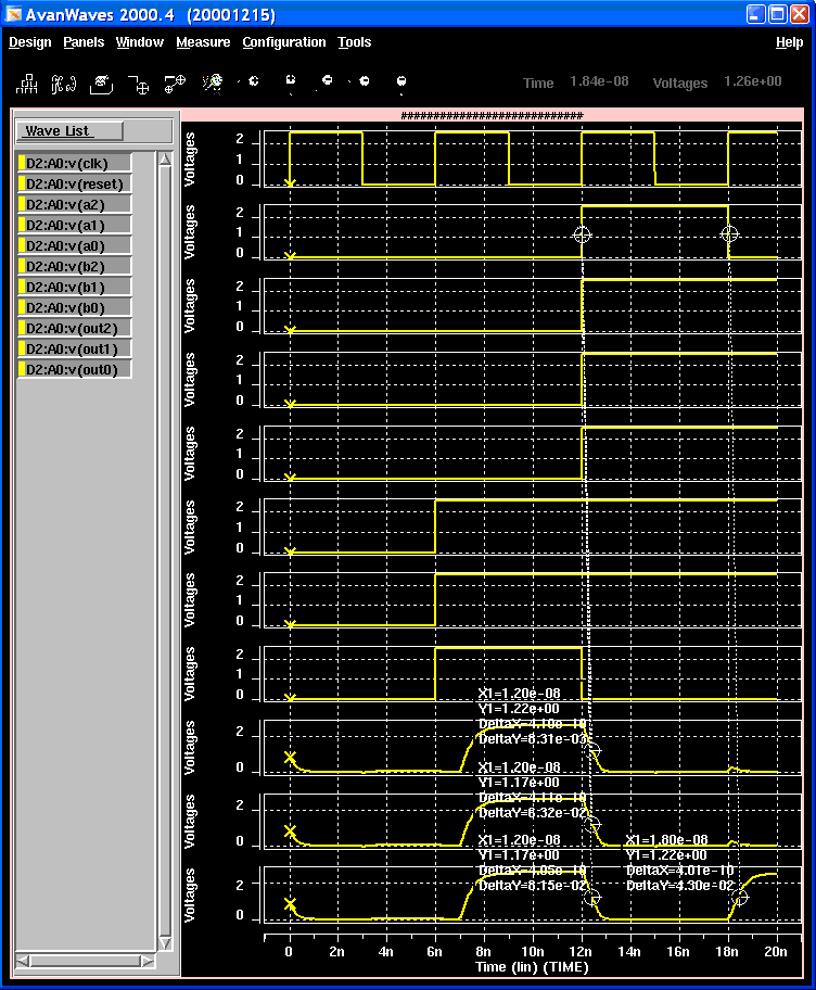
The transitions of Out (out2,out1,out0) are entirely determined by the edge of reset signal.
tpHL=410ps, tpLH=401ps
so tp=(tpHL+tpLH)/2=405.5ps
¡¡
¡¡
Section 4: Layout of 3-bit Absolute Difference Value Circuit