Section 6: Analysis for Critical path and clock frequency:
To measure to worst case delay of out1,out2,out from Ain and Bin, we use the following two cases to achieve the critical path:
case 1:
Every bit of Dout3 changes from 1 to 0, we use the input combination (Ain,Bin) 111 110 -> 000 111 to obtain this.
This can be verified using the function of the comparator: Dout3=Bi’*Ai + Bi’*Cin3 + Ai*Cin3
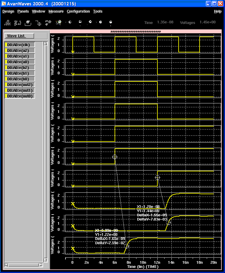
Since both Ain (a2,a1,a0) and Bin (b2,b1,b0) transit at the same edge, so we can pick up one edge of input signals to measure the worst case propagation delay of Out,
tp_out0=1.65ns, tp_out2=tp_out1=1.55ns
So the average tp_out= (1.65+1.55+1.55)/3= 1.58ns
case 2:
Every bit of Dout3 changes from 0 to 1, we use the input combination (Ain,Bin) 000 111 -> 111 110 to obtain this.
This can also be verified using the function of the comparator: Dout3=Bi’*Ai + Bi’*Cin3 + Ai*Cin3
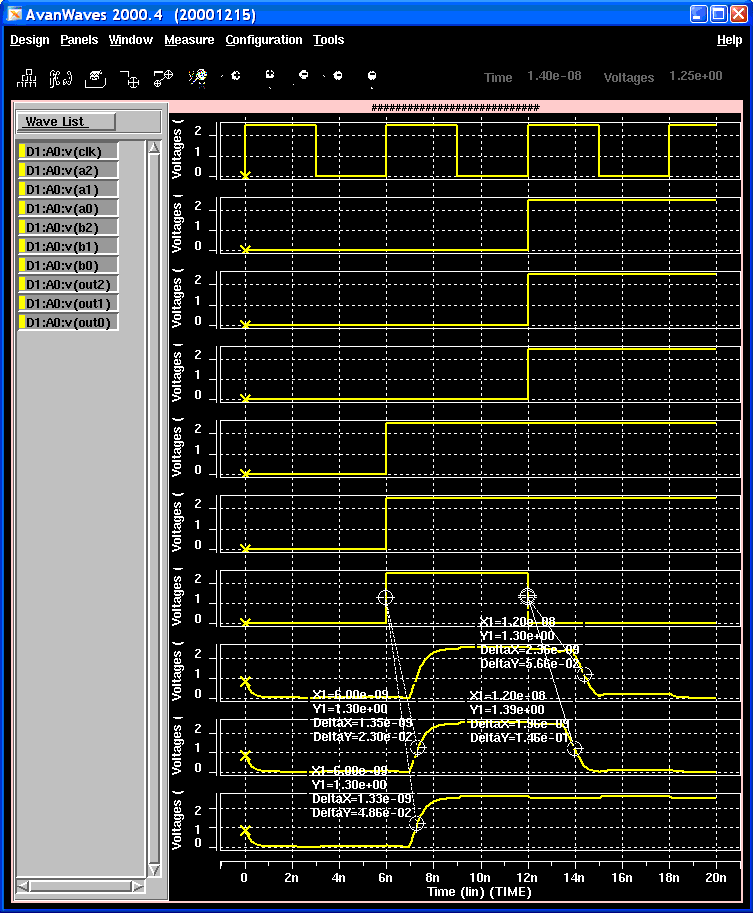
Since both Ain (a2,a1,a0) and Bin (b2,b1,b0) transit at the same edge, so we can pick up one edge of input signals to measure the worst case propagation delay of Out,
tp_out0=1.33ns;tp_out1=(1.35+1.36)/2=1.355ns; tp_out2=(1.35+2.36)/2=1.86ns
So the average tp_out= (1.33+1.355+1.86)/3= 1.515ns
Clock frequency:
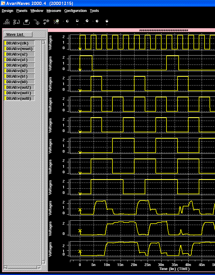
Now we will find the maximum clock frequency of this 3-bit circuit. We need to make sure Out2, Out1, Out0 can fully charge (90% Vdd) and discharge (10%Vdd)when it is maximum frequency.
The waveform below is the waveform when the clock rate rate T=6ns (f=167Mhz). We can see that the output signals meet the requirement: charging and discharging fully.

The waveform below is the waveform when clock rate T= 4ns. We can see that the output waveform is not desirable. Especially the third high level of "out2", it is not charged to 90% of the Vdd. So we can say f=250MHz(T=4ns) is more than the maximum frequency of this circuit could be.
After several trial and error simulation, I found that T=4.7ns is the lowest clock period to make the output signals fully charge and discharge. The waveform for T=4.7ns is shown below. So the maximum frequency of the 3-bit Absolute Difference Value circuit is f= 213MHz

Section 7: Power Consumption for the Absolute Difference Value Circuit (HSPICE)