PROJECTS
![]()
PROJECTS
![]()
1. High-speed A/D converters in low-voltage standard CMOS processes:
This project focuses on the development of low-voltage, high-speed data converters implemented in standard and mixed-signal CMOS processes. As one of the bottlenecks of low-voltage, mixed-mode IC design is represented by the availability of true low-voltage analog circuitry, our research is proposing new circuit design techniques to override the limitations of deep sub-micron CMOS technology that are encountered in the design of analog cells. The project has two major tasks:A. Implementation of a continuous-time Delta-Sigma modulator for next generation wireless devices;A. Low-voltage continuous-time Delta-Sigma modulators:
B. Design of a low-latency high-speed A/D converter using folding and interpolation techniques.Continuous-time implementations of Delta-Sigma modulators have several advantages compared to SC realizations: less power hungry, less prone to pick up digital noise, easy to drive from external sources, can operate at higher sampling frequencies, the errors of the S/H circuit are shaped by the loop filter. However, in literature there are only few reported CMOS realizations of low-pass continuous-time Delta-Sigma modulators. Our preliminary results envisage that a proposed target of 12.5bit resolution at a bandwidth of 2.5MHz can be achieved with a continuous-time implementation operating a single supply voltage of 1.8V and dissipating less than 10mW. (See figure below; click on figure to enlarge it)
 |
B. Low-voltage folding and interpolating A/D converter:
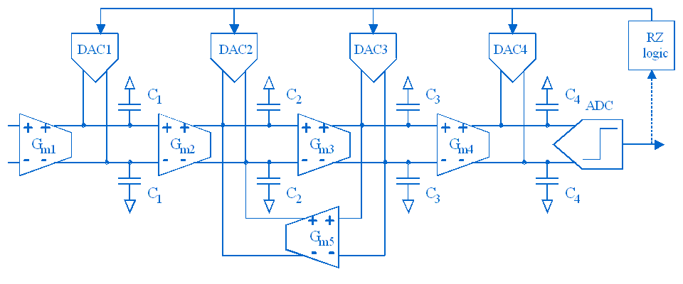
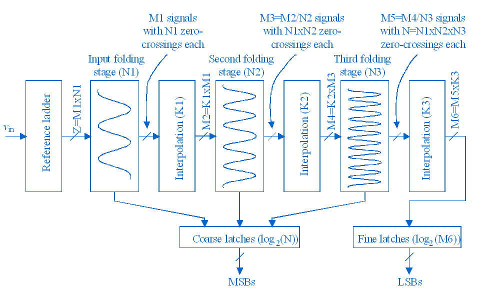
The second research topic for this project is regarding the possibility of obtaining a high-speed (100MS/s), medium resolution (10 bits), low-latency (no pipelined) A/D converter in a standard (without linear capacitors) low-voltage (2.5V) CMOS process. The folding architecture is an alternative approach to avoid the complexity of the flash converter that increases exponentially with the resolution. The folding A/D topology has the speed of the flash ADC, while the number of comparators is greatly reduced with analog preprocessing. Reducing the number of folding blocks through interpolation can further decrease the power consumption of such a converter.
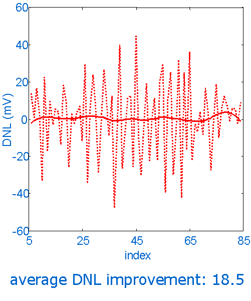
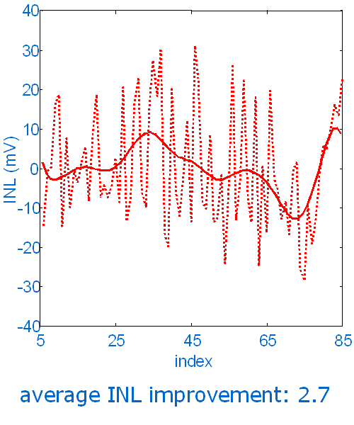
Device mismatch limits the INL and DNL in standard design architecture for flash and folding A/D converters and it is a fundamental drawback in making high-resolution converters. We proposed an active spatial filter, using negative resistors implemented with Negative Impedance Converters, to reduce INL and DNL errors. (See figures below; click on figure to enlarge it)
 |
 |
 |
2. SOI CMOS
Continuous-Time Delta-Sigma A/D Converters for Space Communication Radio
Receivers
Silicon-on-Insulator (SOI) CMOS technology is one of the options for the future in the International Technology Roadmap for Semiconductors (ITRS), based on the anticipated economic benefit. Bulk CMOS is still clearly the mainstream choice for most applications, but considerable advances in SOI technologies have allowed fabrication of impressive circuits and devices, especially for the use in harsh environments and low-voltage/low-power applications. However, because SOI has not become a mainstream CMOS, although being under consideration for almost three decades, there is a considerable lack of design techniques and available standard cells (especially analog) for SOI CMOS mixed-signal integrated circuits. The research effort we are proposing for this project will be focused on developing a set of such analog cells, specifically Delta-Sigma A/D converters, to be used in radioreceivers for space communications.
Delta-Sigma oversampling A/D converters realize an optimum trade-off between circuit complexity, cost, and power dissipation, high accuracy being achieved with low precision analog components. Continuous-time implementations of Delta-Sigma modulators have already proven to offer the advantages of lower power consumption and higher frequency operation compared to switched-capacitor counterparts. We also envisage, based on the fact that CT realizations do not fold high frequency perturbations back into the signal band, that radiation effects (especially single eventstransients) will not affect to a great extent their performance. Combined with the advantages brought by the SOI CMOS technology we expect to obtain extremely low-power, wide bandwidth, radiation immune A/D converters.
![]()
Home | Research | Projects | Publications | Members | Facilities | Map | Links