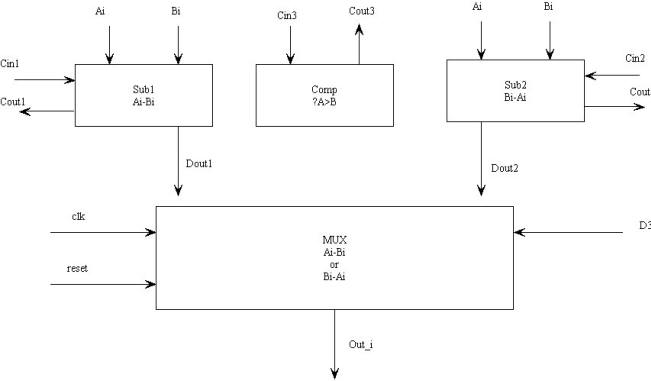
Section 1: Schematic of The Absolute Difference Value Circuit
The diagram of one bit slice of AVC is shown below:
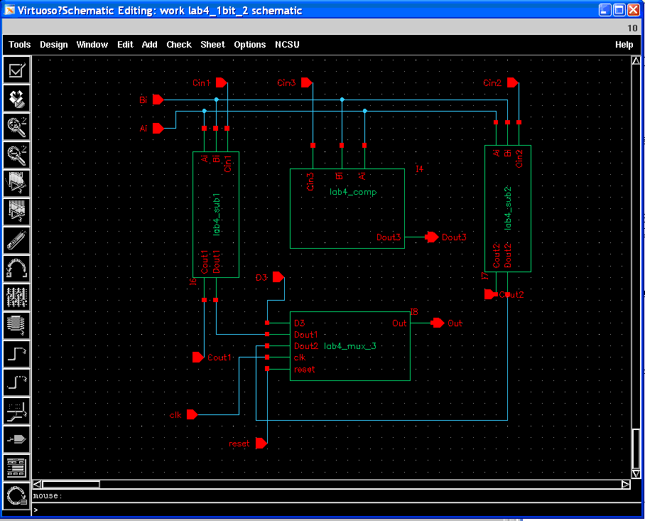
Here we use two subtractors (Sub1 and Sub2) to calculate Ai-Bi and Bi-Bi. The comparator is to determine if Ai>Bi or Bi>Ai. After determining all the N bits, the comparator gives the MUX a feed back: D3, to select either the result of Sub1 or Sub2.
Sub1 and Sub2 have the same input Ai Bi, the borrow carrier from the previous bit slice Cin1 and Cin2; they also have two outputs: the difference value: Dout1 and Dout2 and the borrow carrier for the next bit slice Cout1 and Cout2.
Dout1=Ai¨’Bi¨’Cin1
Dout2=Ai¨’Bi¨’Cin2
Cout1=Ai¡¯*Bi + Ai¡¯*C1i + Bi*Cin1
Cout2=Bi¡¯*Cin2 + Bi¡¯*Ai + Ai*Cin2
¡¡
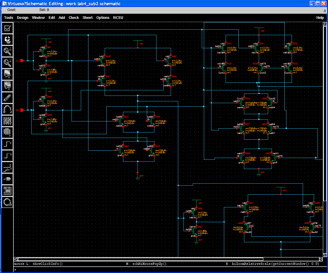
The Schematics of the absolute value circuit are shown below:
¡¡
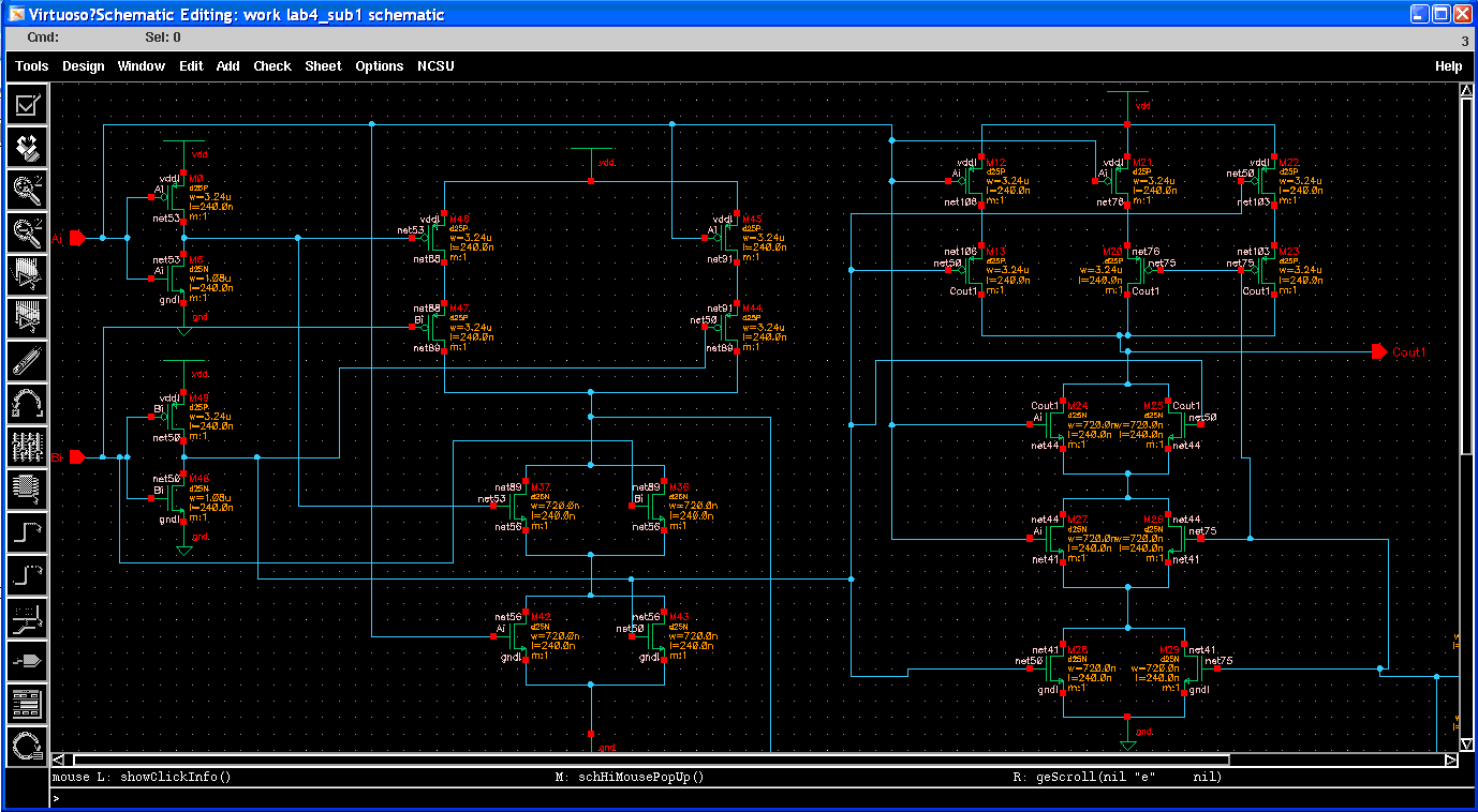
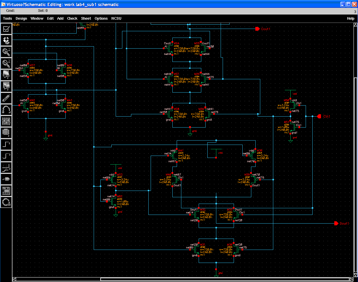
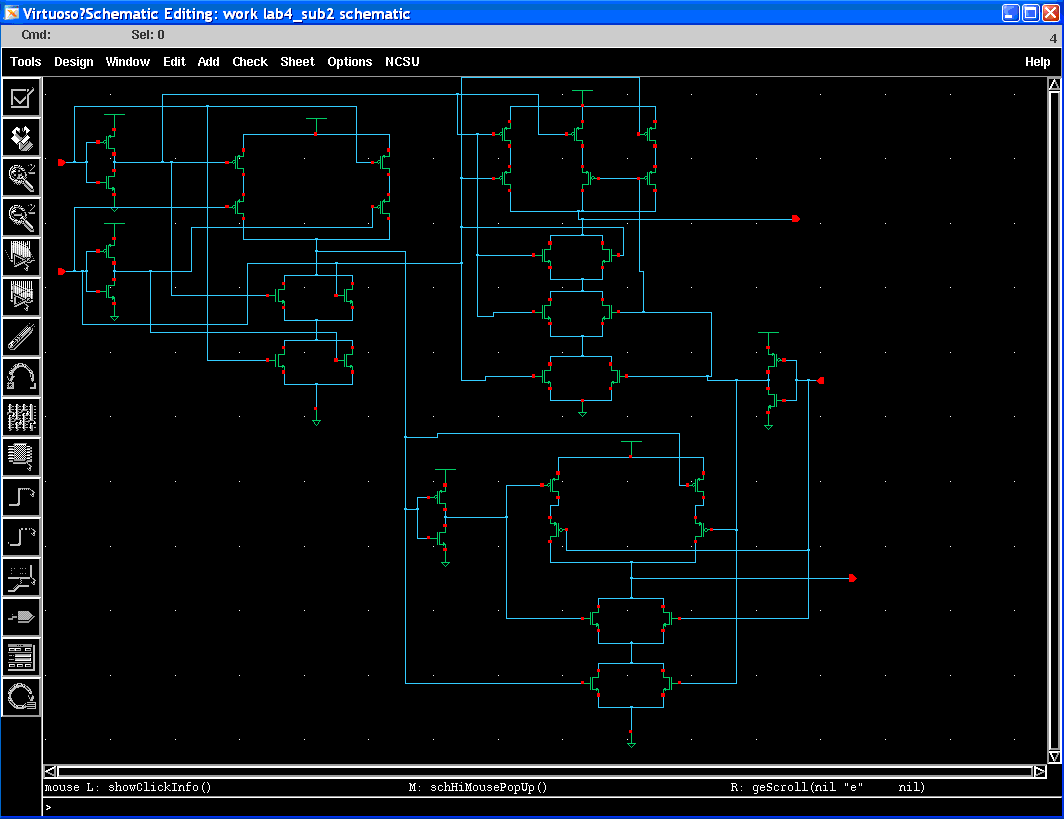
Sub1:
Sub1 is designed using static CMOS design, two more detailed circuits are shown below. The section which generates Dout1 is a three-input(Ai,Bi and Cin1) XOR circuit, and the section which generates Cout1 is to realize the function: Cout1=Ai¡¯*Bi + Ai¡¯*C1i + Bi*Cin1
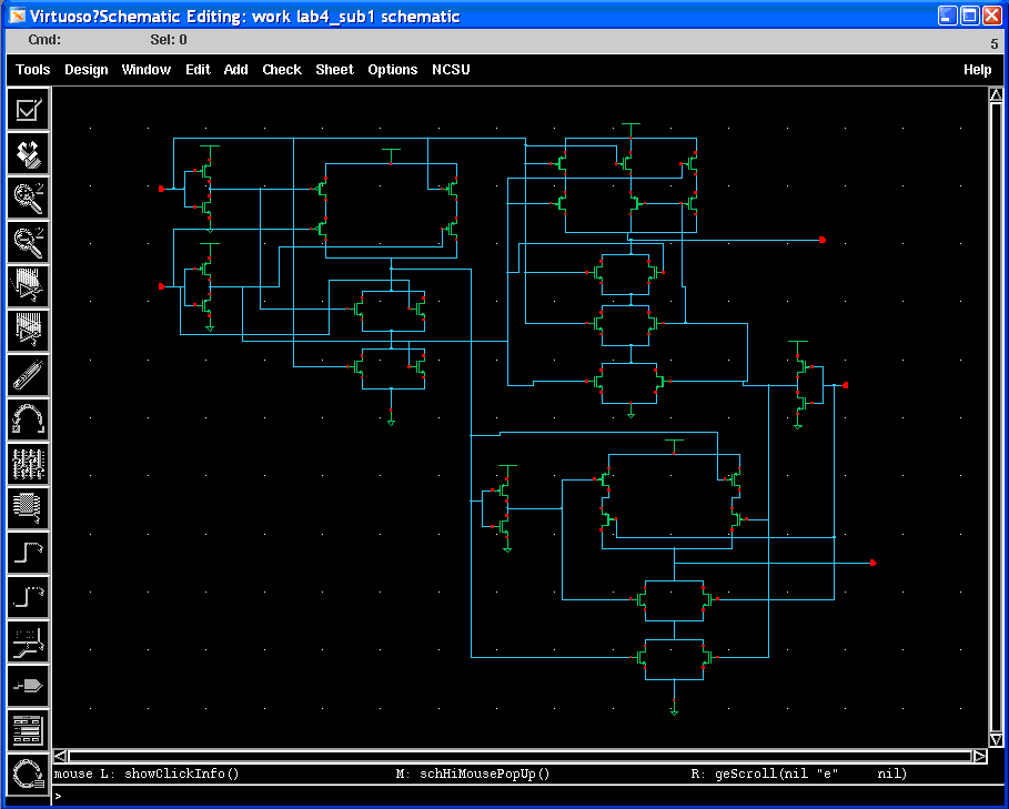
Two detailed schematics:
Part1:
¡¡
Part2:
¡¡
¡¡
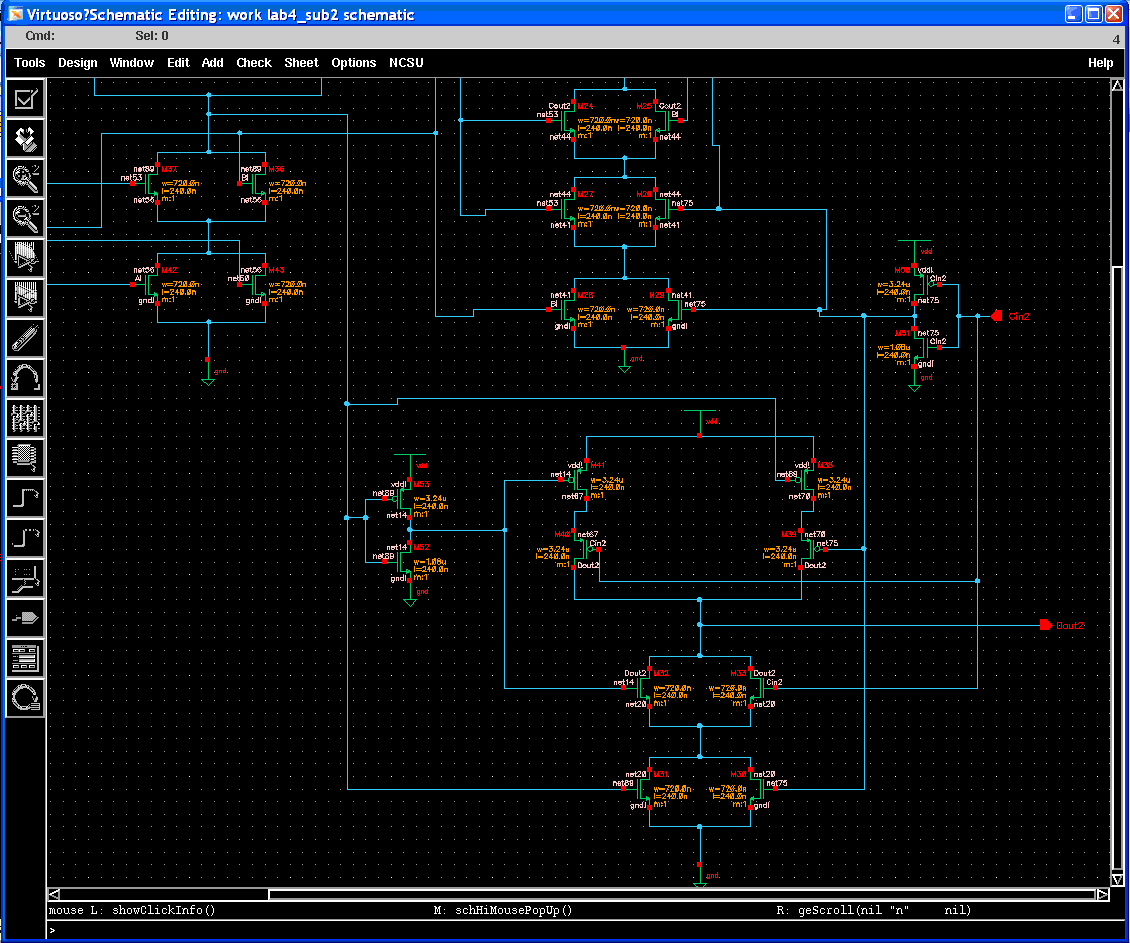
Sub2:
The circuit of Sub2 is similar to Sub1, the circuit realizes the following two functions:
Dout2=Ai¨’Bi¨’Cin2;
Cout2=Bi¡¯*Cin2 + Bi¡¯*Ai + Ai*Cin2
¡¡
¡¡
¡¡
¡¡
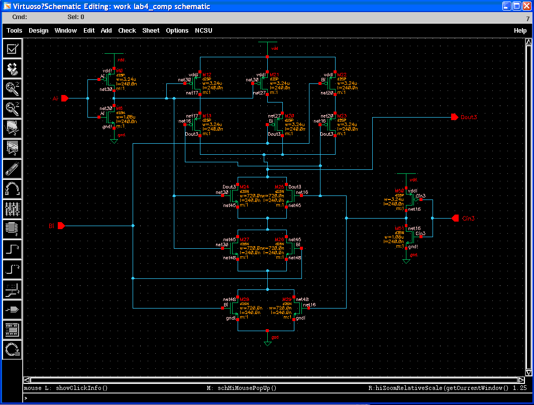
Comparator:
The Comparator is to determine which input is larger before doing subtraction. It has three inputs: Ai, Bi and Cin3, it also has one output: Dout3. The comparator starts from LSM to MSB, if Ai>Bi, then Dout3=1; if Ai<Bi, then Dout3=0; if Ai=Bi, then Dout3 = Cout3. The function is as below:
Dout3=Bi¡¯*Ai + Bi¡¯*Cin3 + Ai*Cin3
The schematic is shown below. The comparator is also designed using static CMOS circuit.
¡¡
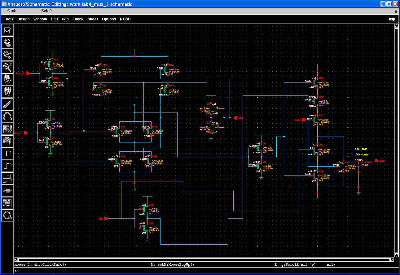
MUX:
The inputs of MUX circuit are Dout1, Dout2, D3, clk and reset, the output is Out. After finishing comparing all the N-bit of A and B, if A>B, the output of the MUX for this bit slice is the result of Sub1: Dout1 = Ai-Bi; if A<=B, the output of the MUX for this bit slice is the result of Sub2: Dout2 = Bi-Ai; The function is: Out = Dout2*D3'+ Dout1*D3
¡¡
I also put a positive level-sensitive latch in the MUX circuit, which is shown in the picture below. When the clk is high, the output can pass through the latch. Besides the clk signal, the Positive latch also has a reset signal, which can reset the output to 0 when necessary.
¡¡
¡¡
¡¡
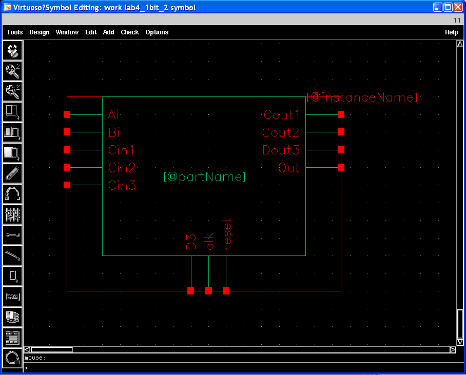
One-bit Symbol of the Absolute Difference Value Circuit:
Combining the above parts together, we can get the 1-bit slice of the circuit, which is shown below.
¡¡
Following is the symbol of the one-bit slice:
¡¡
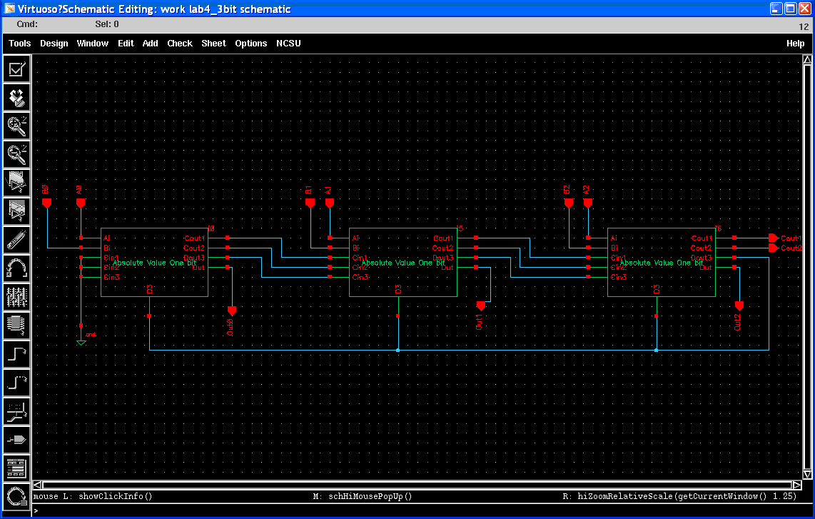
Using the one-bit slice ,we can obtain the schematics for the N-bit Absolute Difference Value Circuit, following is a 3-bit circuit, our following analysis will be based on this 3-bit circuit. Note when expanding this 3-bit circuit into N-bit circuit, the input of D3 should be the output of Dout of the MSB. It means after comparing the two inputs, the comparator in the MSB tells each of the three bits which one is larger and then they can do the subtraction.
¡¡