Section 2: Schematic Functionality Verification (IRSIM):
After the schematic was completed, the functionality was verified in IRSIM. The following was created with the following IRSIM command file:
|sim.cmd stepsize 50
vector Ain A2 A1 A0
vector Bin B2 B1 B0
vector in clk reset
vector Out Out2 Out1 Out0
analyzer clk reset Ain Bin Out
set Ain 111
set Bin 000
set in 10
s
set Ain 111
set Bin 000
set in 00
s
set Ain 000
set Bin 000
set in 10
s
set Ain 000
set Bin 000
set in 00
s
set Ain 001
set Bin 000
set in 10
s
set Ain 001
set Bin 000
set in 00
s
set Ain 000
set Bin 111
set in 10
s
set Ain 000
set Bin 111
set in 00
s
set Ain 111
set Bin 110
set in 10
s
set Ain 111
set Bin 110
set in 00
s
set Ain 000
set Bin 001
set in 11
s
set Ain 000
set Bin 001
set in 01
s
set Ain 011
set Bin 000
set in 10
s
set Ain 011
set Bin 000
set in 00
s
set Ain 000
set Bin 000
set in 10
s
set Ain 000
set Bin 000
set in 00
s
set Ain 101
set Bin 010
set in 10
s
set Ain 101
set Bin 010
set in 00
s
set Ain 010
set Bin 101
set in 10
s
set Ain 010
set Bin 101
set in 00
s
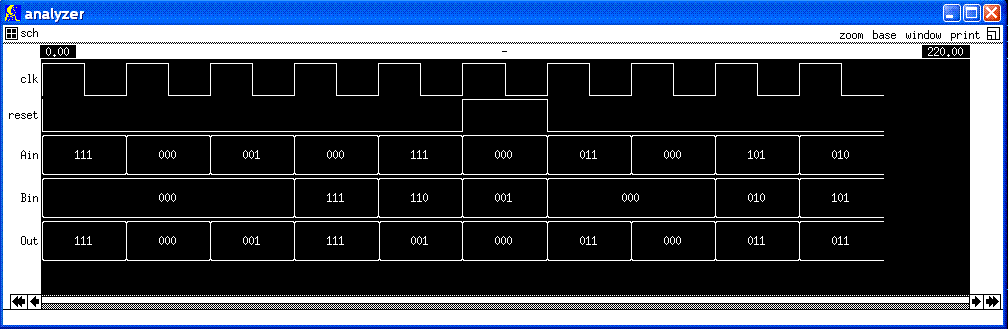
As we can see in the above waveform, the logic of the circuit turns out exactly as we expected. The output is the absolute difference of the input Ain and Bin. And when the reset becomes high, the out will become 000 no matter what the input Ain and Bin are.
Section 3: Propagation delay analysis of schematics