Section 5: Layout Verification (IRSIM and HSPICE)
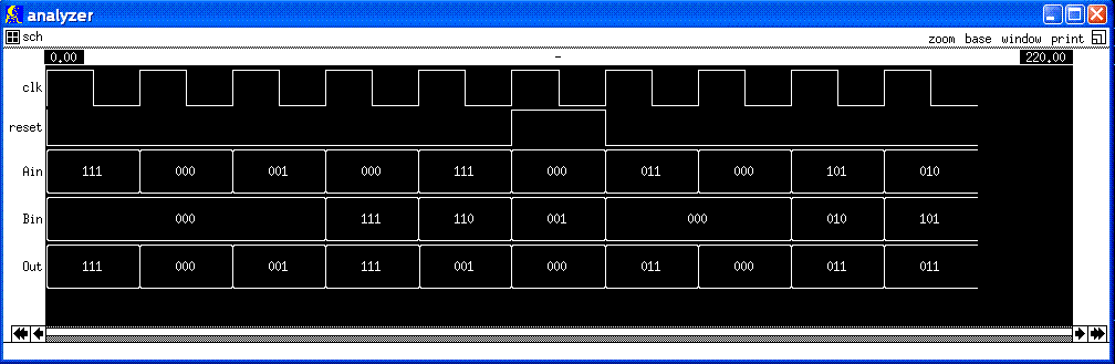
After the layout was completed, it was verified using IRSIM and HSPICE. The following IRSIM waveform was done with the IRSIM command file.
When the reset becomes high, the out of each bit slice will become 0, whatever the input Ain and Bin are.
The HSPICE simulation is shown below using the spice file. The load capacitance at the output is 50fF.

As we can see in the waveform, the circuit works exactly as a Absolute Difference Value calculator with reset signal. For example: right after reset becoming 0, Ain=111, Bin=011, the output is 100, then Ain=000, Bin=011, the output becomes 011.
Rise and Fall time:
The rise and fall time of Out2 is shown below:
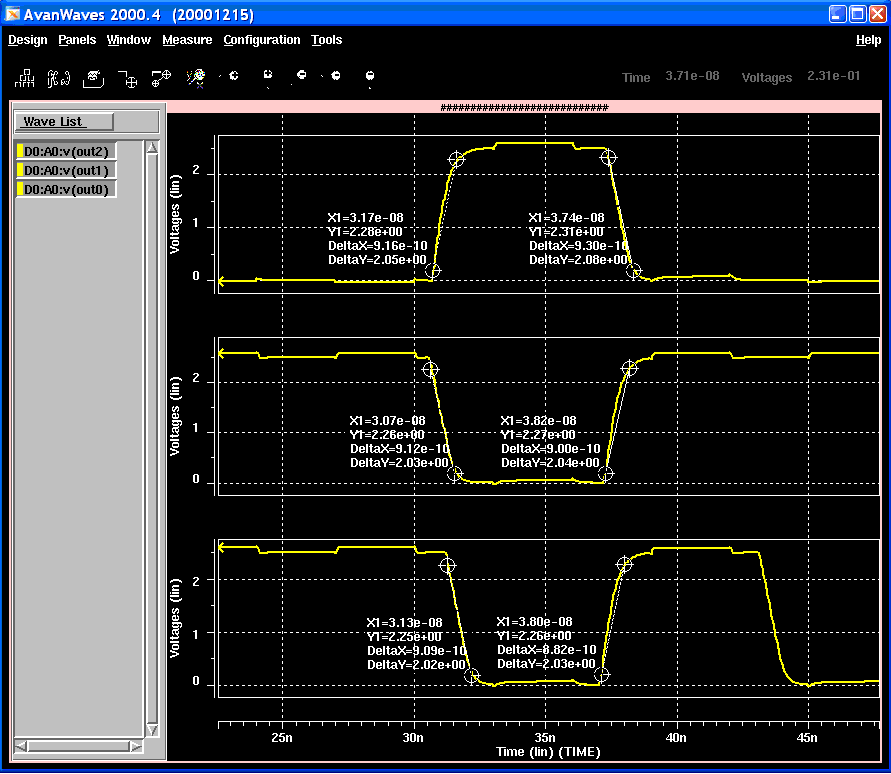
Tr_out2=908ps, Tf_out2=916ps
Tr_out1=912ps, Tf_out1=900ps
Tr_out0=909ps, Tf_out2=882ps
Since the bit slice structures of the 3 bits are identical, it is reasonable that they have close rise times and fall times
Section 6: Critical path and clock frequency for the absolute difference value Circuit (HSPICE)