Back | Previous
project | Next project
| GaInAsSb/GaSb and GaInAsSb/AlGaAsSb Heterostructures
for TPV applications |
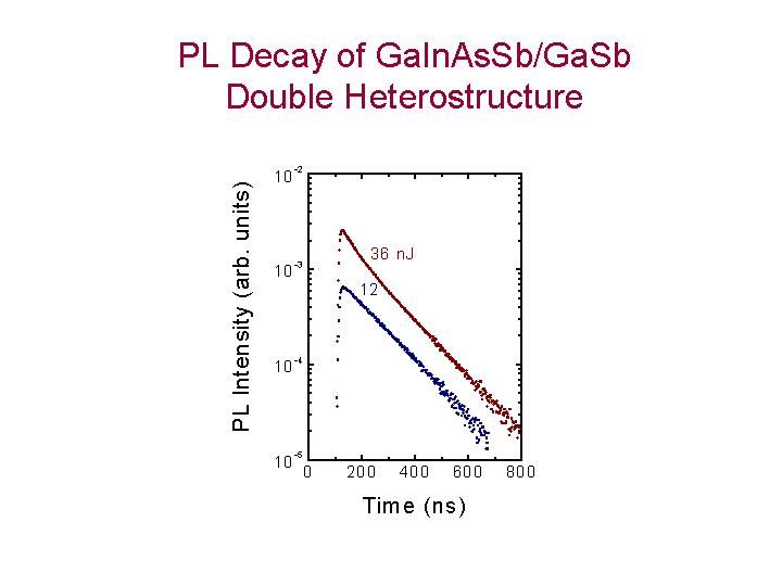
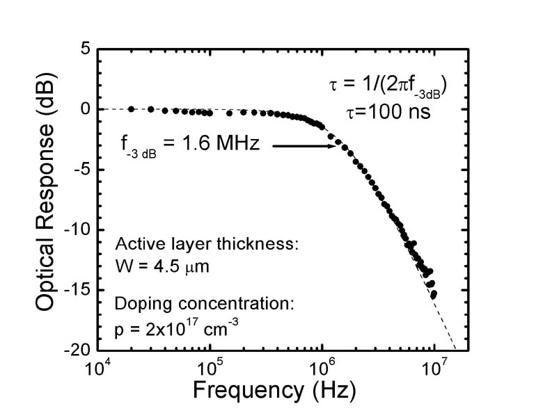
Minority carrier lifetimes in 0.55-eV band-gap GaInAsSb epitaxial layers
that are double capped with GaSb or AlGaAsSb layers were determined using
time-resolved photoluminescence and modulation
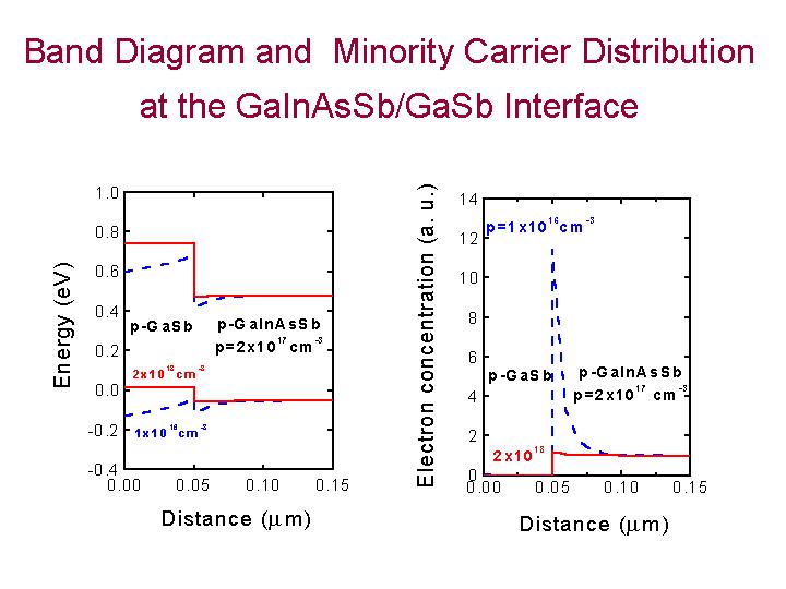
response to sinusoidal excitation. It was found that accumulation
of electrons at the p-doped GaInAsSb/GaSb type-II interface contributes
significantly to the interfacial recombination velocity (S), which was
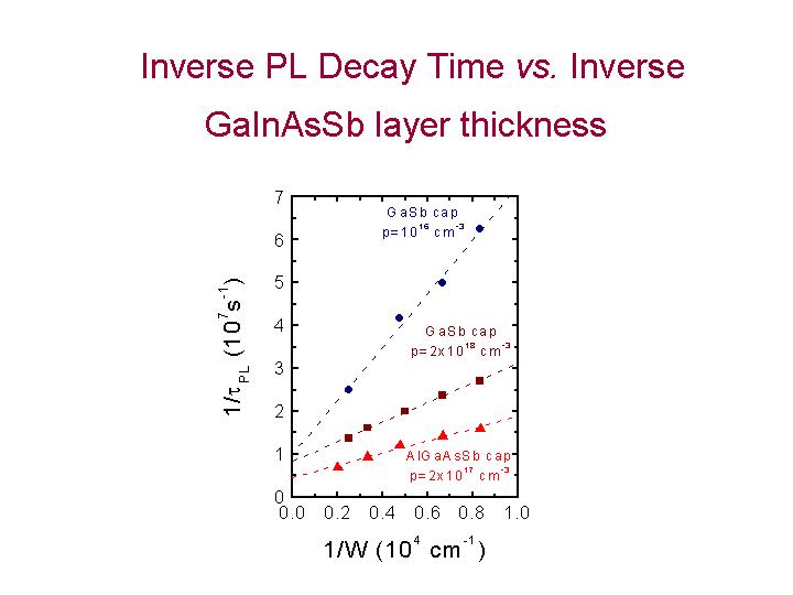
measured to be 3100 cm/s. The use of heavily p-doped GaSb cap layers was
proposed to eliminate the potential well for electrons
and barrier for holes at the interface. Increasing the GaSb cap doping
level from 1 × 1016 cm-3 to 2 × 10¹⁸
cm-3 resulted in a 2.7 times reduction
of S down to 1140 cm/s. The smallest value of S
was determined to be 720 cm/s, which was obtained for structures with AlGaAsSb
cap layers that have no valence band offset.