ESE 545 Project
A dual-issue Cell SPU-lite pipelined multimedia processor and its VHDL/Verilog/SystemVerilog model
The goals of the project are to:
1) learn multimedia processor design using Sony Cell processor architecture and its implementation as an example;
2) develop your own (simplified) model of a dual-issue pipelined multimedia processor architecture and its VHDL/Verilog implementation.
Below are the links where you find necessary information about the SONY Cell processor architecture and its first implementation:
1. Cell architecture and its first implementation (2005) , (2006)
2. Synergistic Processor Unit (SPU) Instruction Set Architecture v.1.2
The required reading are Cell implementation (2006) and SPU ISA.
It is a one or two students per team.
All critical steps of the processor model design project will be discussed during lectures so do not panic if you do not have the complete knowledge of how to do it at the start of the class!
Based on the feedback from the former ESE 545 students, this project helped many of them to get a good job in computer firms, such as Intel, AMD, ARM, Broadcom, Samsung, Qualcomm, Nvidia, Apple, etc.
Below is the project implementation schedule.
Step 1. Learn Sony Cell SPU instruction set architecture (SPU ISA) and its implementation and refresh your knowledge of CAD tools for VHDL, Verilog/SystemVerilog-based design.
I. As an example, look how the Verilog code is used to describe the operation of the 5-stage MIPS pipeline. The MIPS architecture and its pipelined implementation as well as data forwarding will be discussed in the class.
II. There are two HDL simulators available at the lab: QuestaSim (Siemens) (used in ESE 507) and Xcelium (Cadence).
For those who are going to use QuestaSim, here is the short tutorial written by Prof. Peter Milder who kindly shared it with us.
III. To use Xcelium, read and do the following.
export JAVA_HOME=/usr/lib/jvm/java-1.
export CDS_LICENSE_FILE=5280license4.
if [ -z "$LM_LICENSE_FILE" ]; then
export LM_LICENSE_FILE=5280@license4.
else
export LM_LICENSE_FILE=${LM_LICENSE_
fi
export XCELIUM_HOME=/usr/local/cds/
export VERISIUM_DEBUG_ROOT=/usr/local/
export CDA_ASSISTANT_HOME=/usr/local/
export QUESTASIM_HOME=/usr/local/mgc/questasim
export CDA_DOC=$XCELIUM_HOME/doc/:$VERISIUMDEBUG_ROOT/doc:$CDA_DOC
export PATH
After the changes are done, save your .bashrc file.
After a new login to one of the lab computers, switch to bash by executing 'bash' command.
Check whether everything is set correctly by executing: (to be done once)
which xrun
If you see "/usr/local/cds/XCELIUM2409/tools.lnx86/bin/xrun", then the settings for Xcelium are done correctly.
Create your design directory.
When cda gui is running, search for "Introduction to the Xcelium Simulator"
IV. Cell SPU microarchitecture. Read Cell implementation (2006) and SPU ISA.
By the end of this preparation step, you are expected to get:
- Basic knowledge of multimedia SIMD instructions operating on multiple packed operands and CELL SPU instruction set.
- Knowledge of modern CAD tools, e.g. Cadence or ModelSim (Mentor Graphics) or other.
Step 1. Define your instruction set (a subset of Cell SPU instructions) and develop & test the VHDL/Verilog/SystemVerilog model of a processing core that included a Register file,
data forwarding circuits, and two pipes each with multiple pipelined processing units (including local memory) for your processor
(to be discussed with Instructor first in person no later than 11:00 AM Feb. 18, 2026)
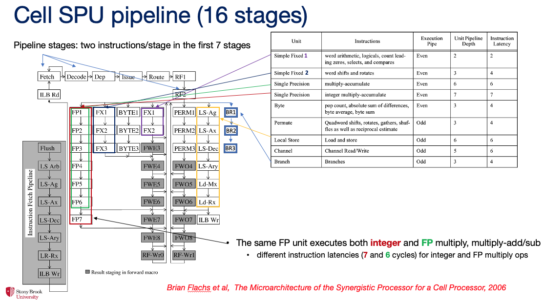
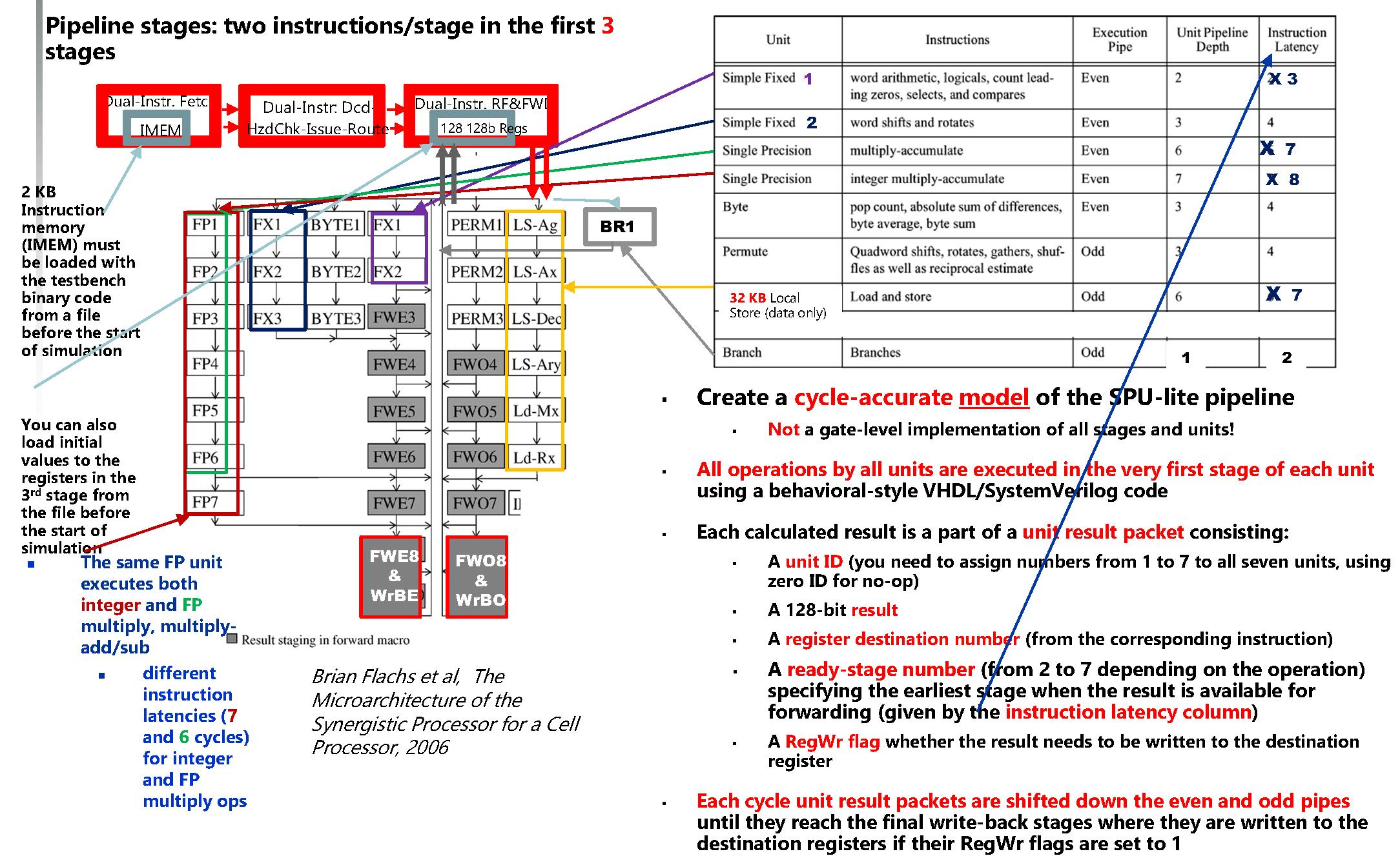
ESE 545 SPU-lite pipeline (11 stages)
By the end of this Step 1, you will need to deliver the following:
- (Delivery # for Step 1: Instruction Set Table report) Define your model Cell SPU-lite instruction set (a subset of ~90-100 SONY Cell SPU instructions) and put it into a table that has the following format:
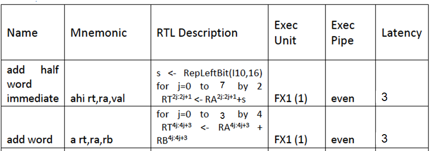
Each Exec Unit field shows the SPU unit name (e.g., FX1 for a Simple Fixed unit 1) and its unique ID (1) that you needs to assign to it. There are seven units, so the numbers from 1 through 7 needs to be used, while reserving unit ID = 0 for no-op operations (empty cycles).
Latency comes from the Instruction Latency column for a corresponding unit (see next/above Figure). This value shows at which cycle from the start of execution the unit result becomes ready for forwarding to other (dependent on it) operations in the even and odd pipes. So, the earliest time when any operation can use a result of a add word instruction is two cycles after the start of execution of the add word operation in the even pipe.
To do that you have to do the following: a) include the basic sub-set of set general-purpose RISC architecture operations (to be discussed in the class); b) figure out what other operations and packed data types need to be included to add multimedia capabilities (should be discussed and confirmed during Instructor's office hours by every team).
Deadline for Delivery for Phase 1 (your instruction set table) report): 11:00 PM Feb. 19 by email to Instructor.
Step 2: Develop and Verify by simulation VHDL/Verilog/SystemVerilog pipeline models of two processing pipes, register file, and forwarding circuits in SPU.
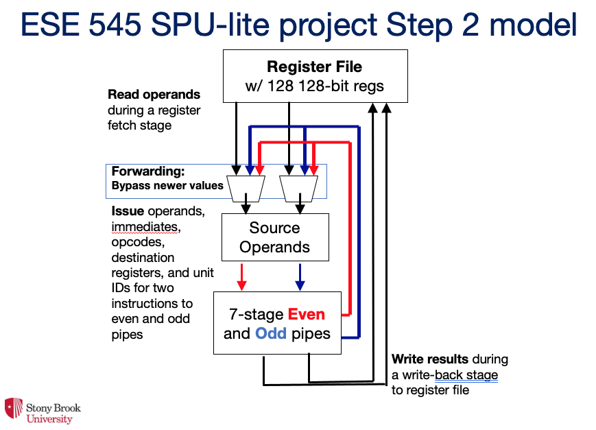
Each pipe can receive and complete one operation per cycle (one/pipe) and forward all calculated results from its intermediate stages, when necessary. The register file latency must be 1 cycle (rather than 2 as in SPU). All units in the pipes must have the same latencies (in cycles) as in SPU. The VHDL code of operations in the units within the pipes is to be developed using behavioral style coding. There is absolutely NO need to develop internal unit structure and its gate-level implementation. The only difference with SPU ISA is the branch operation implementation. Rather than implementing the SPU compiler-assisted branch implementation using branch hint operations, you will need to choose ither static (predict-not-taken) or dynamic branch prediction for your model.
Delivery for Phase 2: The 9-stage SPU-lite HDL Datapath Implementation and Verification
Deadline for Delivery for Phase 2: 11:00 PM March 29, 2026 by email to Instructor.
- Submit (by email) a report (with a description of the work, structural diagrams, a VHDL/Verilog code and simulation results included) showing the set of pipelined units, their set of operations, the number of pipeline stages, VHDL/Verilog code, and testing results.
The successful and timely completion of Step 2 earns you up to 25% (out of 50%) of points for the project.
Step 3. Develop a complete dual-issue 11-stage pipelined processor model
Subtasks:
1)
develop
a dual-issue pipelined version of the multi-stage
pipelined multimedia processor shown above (with local memory as a part of its
load/store unit as in SPU) in VHDL/Verilog/SystemVerilog.
2)
verify your design with a set of test (assembly-level) programs;
3)
document the results of this step to be presented later in a separate
section of your report.
Deadline for Step 3: 1:00 PM May 3, 2026 Final report to be submitted by email to Instructor
1)
prepare and submit a electronic version of your report that must include a
description of your project, goals, design decisions, source code for the
parser and the simulation model, all simulation results to prove that your
model executes correctly all the tasks described in a separate Project
Summary Table;
2) prepare and submit a filled-in
Project Summary
Table.
Step 4. Project presentation by each team to Instructor in the graduate (room 183) or undergraduate (room 246) Linux labs: May 4, 2026 (TBD)
Every team should be prepared to give a ~30-35-minute presentation (no slides necessary!) & answer questions from Instructor during the presentation using lab computers only (not your personal computers!).
The project will be graded based on:
1)
substance of the project (originality, complexity, and completeness of all
Steps),
2)
quality of the report.
Good luck!
Additional notes:
|