In Lab 4, we will design an Absolute Difference Value Circuit (AVC) which calculate the absolute value of the difference of two inputs. I came up this idea when I was learning the pipelining in Chapter 7 and meet a circuit to calculate |a+b|, so I decided to design an |a-b| circuit.
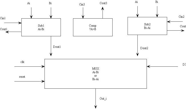
This circuit maybe further used in more complicated computation circuit. It is designed using bit-slice method. One bit slice of AVC consists of two subtractor, one comparator and one MUX.
Using this 1-bit slice, we can obtain the N-bit absolute difference value calculator. In this lab, we mainly focus on the properties of the 3-bit absolute difference value circuit.
Goals for the lab:
The diagram of one bit slice of AVC is shown below:
Lab 4 and Result Links:
Section 1: Schematic of The Absolute Difference Value Circuit
Section 2: Logic Validation of schematic (IRSIM)
Section 3: Propagation delay analysis of separate parts of schematics
Section 4: Layout of 3-bit Absolute Difference Value Circuit
Section 5: Layout Functionality Verification (IRSIM and HSPICE)
Section 6: Critical path and clock frequency for the absolute difference value Circuit (HSPICE)
Section 7: Power Consumption for the Absolute Difference Value Circuit (HSPICE)
Conclusions:
An resettalbe Absolute Difference Value circuit was designed, the bit slice could be used in N-bit circuit.
In this lab, we mainly focused on the properties of 3-bit Absolute Difference Value circuit.
1. Total Area: 0.03mm^2
2. Propagation delays of separate parts was analyzed:
| Sub1 | Sub2 | Comparator | MUX (from select signal D3) | MUX (from reset) | ||
| Dout1 (out) | Cout1(borrow) | Dout2 (out) | Cout2(borrow) | |||
| 287.5ps | 357ps | 287.5ps | 357ps | 562.5ps | 378.5ps | 405.5ps |
3. Critical path was analyzed, the worst case propagation delays of output from the edge of Ain and Bin are:
Case 1: Every bit of Dout3 changes from 1 to 0
tp_out= 1.58ns
Case 2: Every bit of Dout3 changes from 0 to 1
tp_out= 1.515ns
4. Maximum clock frequency f=212Mhz
5. Power consumption of the circuit: P=Vdd*I_max=112.5mW
The delay might seem a little bit large, it is reasonable since the comparator of this circuit is series structure.
The whole circuit design was my own idea. I understand there might be more efficient and mature circuit in the real VLSI industry. However, doing this lab 4 with my own idea and executing my idea is an useful experience for my VLSI study.